HDI PCBs
HDI PCB TECHNOLOGY
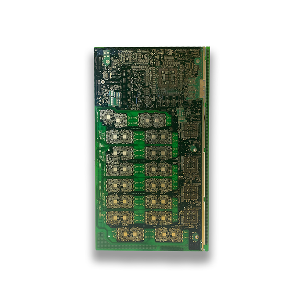
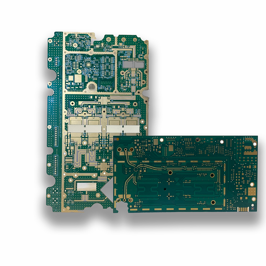
The HDI - High-Density Interconnector PCBs, have a higher wiring density compared with standard PCBs. Building on our experience in manufacturing technology, the PCB Connect Group can support HDI PCB’s up to any layer interconnected technology. For more information on how the PCB Connect Group can advise on your HDI requirement please contact your local PCB Connect business.
| Technology Element | The PCB Connect Group Capability Overview |
|---|---|
| Available Layer Count | 4-40 Layers Standard Capability |
| HDI Construction | 1+N+1, 2+N+2, 3+N+3, 4+N+4, Any Layer Connected (ALIC) |
| Laminate Systems Available | FR4, With Standard & High TG, Low and Ultra Low Loss Dk Laminates, Halogen Free, PTFE |
| Maximum Line Width & Space | 2.5 Mil Minimum Line Width and Space |
| Finished Copper Weight | 18um to 70um |
| Maximum Delivered Panel Dimensions | 600 x 450 As Standard + Backplane Technology |
| Available Surface Finishes | Enig. Immersion Tin, HASL, PB Free HASL, OSP, Heavy Plated Au, Immersion AG, ENEPIG, ASIG, Selective Hard and Soft Gold, Rhodium |
| Smallest Mechanically Laser Drilled Hole Size | 0.10 to 0.07mm Advanced |
| Finished Board Thickness | 0.4 - 6.0mm |
| Solder Mask & Resin Plugged Vias | Solder Mask and Resin Plugged Vias to IPC4761 Type VI |
CONTACT US TODAY TO ASK A SPECIFIC QUESTION

